- 您现在的位置:买卖IC网 > Sheet目录1214 > EVAL-ADE7953EBZ (Analog Devices Inc)BOARD EVAL FOR ADE7953
�� ��
��
��Data� Sheet�
�THEORY� OF� OPERATION�
�ANALOG� INPUTS�
�The� ADE7953� includes� three� analog� inputs� that� form� two� current�
�channels� and� one� voltage� channel.� In� a� standard� configuration,�
�Current� Channel� A� is� used� to� measure� the� phase� current,� and�
�Current� Channel� B� is� used� to� measure� the� neutral� current.� The�
�ADE7953�
�the� voltage� channel� with� gain� options� of� 1,� 2,� 4,� 8,� and� 16� (see�
��The� voltage� channel� gain� is� configured� by� writing� to� the� PGA_V�
�register� (Address� 0x007).� By� default,� the� voltage� channel� PGA� is�
�set� to� 1.�
�voltage� channel� input� measures� the� difference� between� the� phase�
�voltage� and� the� neutral� voltage.� The� ADE7953� can,� however,� be�
�used� with� alternative� voltage� and� current� combinations� as� long� as�
�the� analog� input� specifications� described� in� this� section� are� met.�
�Table� 6.� PGA� Gain� Settings�
�Full-Scale�
�Differential� PGA_IA[2:0]�
�Gain� Input� (mV)� (Addr� 0x008)�
�PGA_IB[2:0]�
�(Addr� 0x009)�
�PGA_V[2:0]�
�(Addr� 0x007)�
�Current� Channel� A�
�Current� Channel� A� is� a� fully� differential� voltage� input� that� is�
�designed� to� be� used� with� a� current� sensor.� This� input� is� driven�
�by� two� pins:� IAP� (Pin� 5)� and� IAN� (Pin� 6).� The� maximum� differ-�
�ential� voltage� that� can� be� applied� to� IAP� and� IAN� is� ±500� mV.�
�A� common-mode� voltage� of� less� than� ±25� mV� is� recommended.�
�1�
�2�
�4�
�8�
�16�
�22�
�±500�
�±250�
�±125�
�±62.5�
�±31.25�
�±22.7�
�000� 1�
�001�
�010�
�011�
�100�
�101�
�000�
�001�
�010�
�011�
�100�
�N/A�
�000�
�001�
�010�
�011�
�100�
�N/A�
�When� a� gain� of� 1� is� selected� on� Current� Channel� A,� the� maximum� pin� input� is�
�LOW-PASS� FILTER�
�FILTER�
�COMPARATOR�
�Common-mode� voltages� in� excess� of� this� recommended� value�
�may� limit� the� available� dynamic� range.� A� programmable� gain�
�amplifier� (PGA)� stage� is� provided� on� Current� Channel� A� with�
��The� maximum� full-scale� input� of� Current� Channel� A� is� ±250� mV�
�when� using� a� single-ended� configuration� and,� therefore,� when�
�using� a� gain� setting� of� 1,� the� dynamic� range� is� limited.� The� Current�
�Channel� A� gain� is� configured� by� writing� to� the� PGA_IA� register�
�(Address� 0x008).� By� default,� the� Current� Channel� A� PGA� is� set�
�to� 1.� A� gain� option� of� 22� is� offered� exclusively� on� Current�
�Channel� A,� allowing� high� accuracy� measurement� for� signals� of�
�very� small� amplitude.� This� configuration� is� particularly� useful�
�when� using� small� value� shunt� resistors� or� Rogowski� coils.�
�Current� Channel� B�
�Current� Channel� B� is� a� fully� differential� voltage� input� that� is�
�designed� to� be� used� with� a� current� sensor.� This� input� is� driven�
�by� two� pins:� IBP� (Pin� 9)� and� IBN� (Pin� 10).� The� maximum� differ-�
�ential� voltage� that� can� be� applied� to� IBP� and� IBN� is� ±500� mV.� A�
�common-mode� voltage� of� less� than� ±25� mV� is� recommended.�
�Common-mode� voltages� in� excess� of� this� recommended� value�
�may� limit� the� available� dynamic� range.� A� PGA� gain� stage� is�
�provided� on� Current� Channel� B� with� gain� options� of� 1,� 2,� 4,� 8,�
�and� 16� (see� Table� 6).� The� Current� Channel� B� gain� is� configured�
�by� writing� to� the� PGA_IB� register� (Address� 0x009).� By� default,�
�the� Current� Channel� B� PGA� is� set� to� 1.�
�Voltage� Channel�
�The� voltage� channel� input� a� full� differential� input� driven� by�
�two� pins:� VP� (Pin� 12)� and� VN� (Pin� 11).� The� voltage� channel�
�is� typically� connected� in� a� single-ended� configuration.� The�
�maximum� single-ended� voltage� that� can� be� applied� to� VP� is�
�±500� mV� with� respect� to� VN.� A� common-mode� voltage� of� less�
�than� ±25� mV� is� recommended.� Common-mode� voltages� in�
�excess� of� this� recommended� value� may� limit� the� dynamic� range�
�capabilities� of� the� ADE7953� .� A� PGA� gain� stage� is� provided� on�
�1�
�limited� to� ±250� mV.� Therefore,� when� using� a� single-ended� configuration,� the�
�maximum� input� is� ±250� mV� with� respect� to� AGND.�
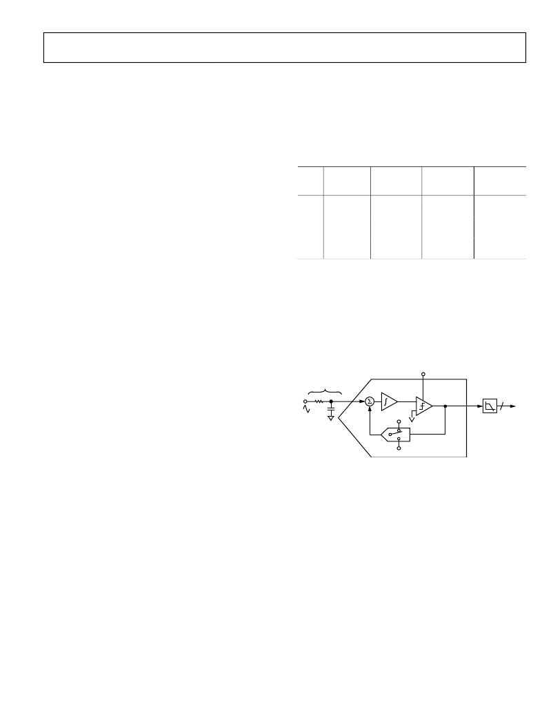
�ANALOG-TO-DIGITAL� CONVERSION�
�The� analog-to-digital� conversion� in� the� ADE7953� is� performed�
�by� three� second-order� Σ-Δ� modulators.� For� the� sake� of� clarity,�
�the� block� diagram� in� Figure� 36� shows� the� operation� of� a� first-�
�order� Σ-Δ� modulator.� The� analog-to-digital� conversion� consists�
�of� a� Σ-Δ� modulator� followed� by� a� low-pass� filter� stage.�
�CLKIN/4�
�ANALOG�
�DIGITAL�
�INTEGRATOR� LOW-PASS�
�LATCHED�
�R� +�
�+�
�–�
�C� –� 24�
�+V� REF�
�.....10100101.....�
�1-BIT� DAC�
�–V� REF�
�Figure� 36.� Σ-Δ� Conversion�
�The� Σ� -Δ� modulator� converts� the� input� signal� into� a� continuous�
�serial� stream� of� 1s� and� 0s� at� a� rate� determined� by� the� sampling�
�clock.� The� ADE7953� sampling� clock� is� equal� to� 895� kHz�
�(CLKIN/4).� The� 1-bit� DAC� in� the� feedback� loop� is� driven� by� the�
�serial� data� stream.� The� DAC� output� is� subtracted� from� the� input�
�signal.� If� the� loop� gain� is� high� enough,� the� average� value� of� the�
�DAC� output� (and,� therefore,� the� bit� stream)� can� approach� that�
�of� the� input� signal� level.� For� any� given� input� value� in� a� single�
�sampling� interval,� the� data� from� the� 1-bit� ADC� is� virtually�
�meaningless.� A� meaningful� result� is� obtained� only� when� a� large�
�number� of� samples� is� averaged.� This� averaging� is� carried� out�
�in� the� second� part� of� the� ADC,� the� digital� low-pass� filter.� By�
�averaging� a� large� number� of� bits� from� the� modulator,� the� low-�
�pass� filter� can� produce� 24-bit� data-words� that� are� proportional�
�to� the� input� signal� level.� The� Σ� -?� converter� uses� two� techniques—�
�oversampling� and� noise� shaping—to� achieve� high� resolution�
�from� what� is� essentially� a� 1-bit� conversion� technique.�
�Rev.� B� |� Page� 19� of� 72�
�发布紧急采购,3分钟左右您将得到回复。
相关PDF资料
EVAL-ADF4002EBZ1
BOARD EVAL FOR ADF4002
EVAL-ADG788EBZ
BOARD EVALUATION FOR ADG788
EVAL-ADM1021AEB
BOARD EVAL FOR ADM1021
EVAL-ADM1023EB
BOARD EVAL FOR ADM1023
EVAL-ADM1031EB
BOARD EVAL FOR ADM1031
EVAL-ADM1062TQEBZ
BOARD EVALUATION FOR ADM1062TQ
EVAL-ADM1075CEBZ
BOARD EVAL FOR ADM1075
EVAL-ADM1087EBZ
BOARD EVALUATION FOR ADM1087
相关代理商/技术参数
EVAL-ADF4001EBZ2
制造商:Analog Devices 功能描述:Evaluation Board For Pll Frequency Synthesizer 制造商:Analog Devices 功能描述:ADF4001 PLL SYNTHESIZER EVAL BOARD
EVAL-ADF4002EB1
制造商:Analog Devices 功能描述:EVAL BOARD - Bulk
EVAL-ADF4002EBZ1
功能描述:BOARD EVAL FOR ADF4002 RoHS:是 类别:编程器,开发系统 >> 评估演示板和套件 系列:- 产品培训模块:Obsolescence Mitigation Program 标准包装:1 系列:- 主要目的:电源管理,电池充电器 嵌入式:否 已用 IC / 零件:MAX8903A 主要属性:1 芯锂离子电池 次要属性:状态 LED 已供物品:板
EVAL-ADF4007EBZ1
功能描述:BOARD EVALUATION FOR ADF4007EB1 RoHS:是 类别:编程器,开发系统 >> 评估演示板和套件 系列:- 标准包装:1 系列:PSoC® 主要目的:电源管理,热管理 嵌入式:- 已用 IC / 零件:- 主要属性:- 次要属性:- 已供物品:板,CD,电源
EVAL-ADF4106EB1
制造商:Analog Devices 功能描述:PLL, Frequency Synthesizer
EVAL-ADF4106EBZ1
功能描述:BOARD EVAL FOR ADF4106 RoHS:是 类别:编程器,开发系统 >> 评估演示板和套件 系列:- 标准包装:1 系列:PSoC® 主要目的:电源管理,热管理 嵌入式:- 已用 IC / 零件:- 主要属性:- 次要属性:- 已供物品:板,CD,电源
EVAL-ADF4108EB1
制造商:AD 制造商全称:Analog Devices 功能描述:PLL Frequency Synthesizer
EVAL-ADF4108EBZ1
制造商:Analog Devices 功能描述:Evaluation Board For ADF4108 制造商:Analog Devices 功能描述:ADF4108 Evaluation Board 制造商:Analog Devices 功能描述:ADF4108, PLL FREQUENCY SYNTHESIZER, EVAL BOARD; Silicon Manufacturer:Analog Devices; Silicon Core Number:ADF4108; Kit Application Type:Clock & Timing; Application Sub Type:PLL Frequency Synthesizer; MCU Supported Families:ADF4108 ;RoHS Compliant: Yes